Flash IntroHomeOur MissionScope of ServicesReference & PartnershipFeedbackContact Us
APDA Technology
Design your solution
A) Substrate Design Feasibility
B) Package Electrical Feasibility
C) Package Thermal Feasibility
D) Package Mechanical Feasibiltiy
E) Packaging Turnkey Solution
A) Substrate Design Feasibility
  • Leading etch packaging design tools
- package feasibility study
 
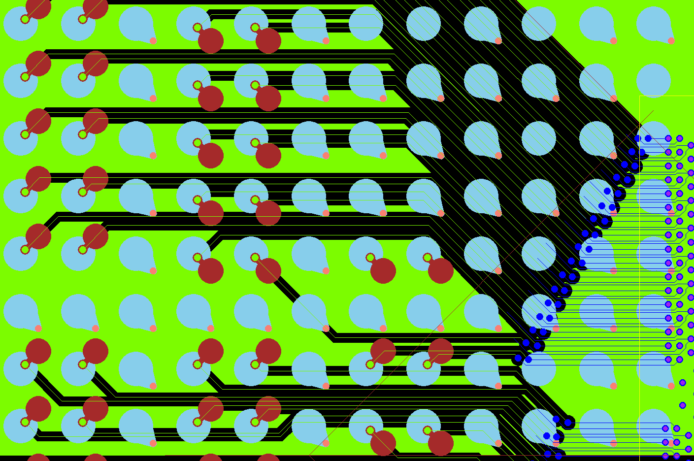
- design on package substrate include leaded, BGA and flip chip package-
  • Support all types of package design
lead frames, laminate, flip chip and module
  • Flexible design rule and substrate technology
tailor make fit customer device and application requirements 
  • Consult and review customer design for manufacturability

APDA Design Flowchart


Flash Intro|Home|Our Mission|Scope of Services|Reference & Partnership|Feedback|Contact Us